
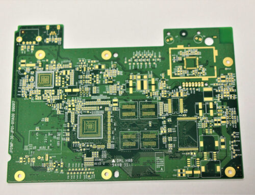
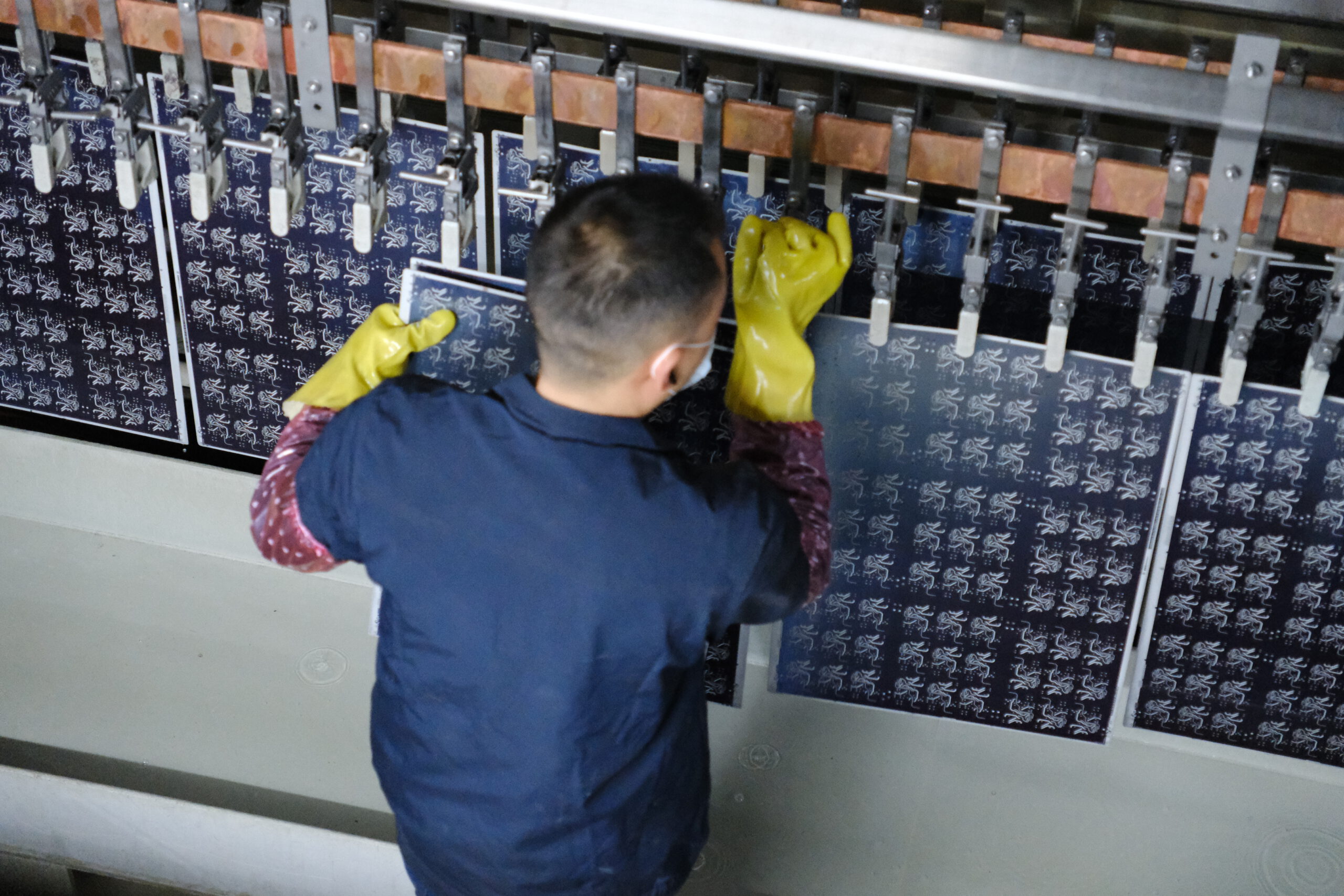
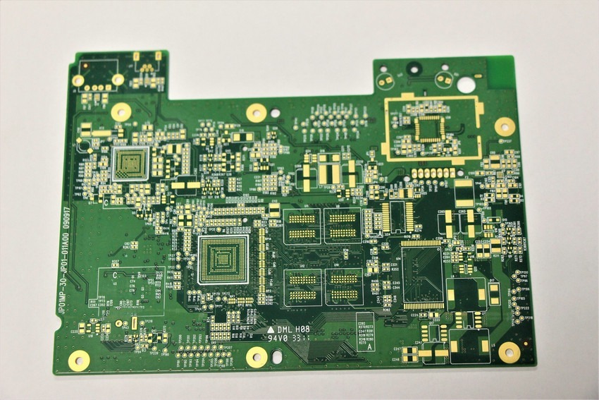
Our Buried Via & HDI PCBs are used in compact, high-speed communication modules, offering signal layer isolation, better space usage, and higher routing density. Perfect for modems, RF modules, and baseband chips where miniaturization and precision matter.
🔹 Applications: Mobile modems, telecom IC modules, IoT basebands
🔹 Features: Blind/buried vias, laser-drilled microvias, fine-pitch routing


")