
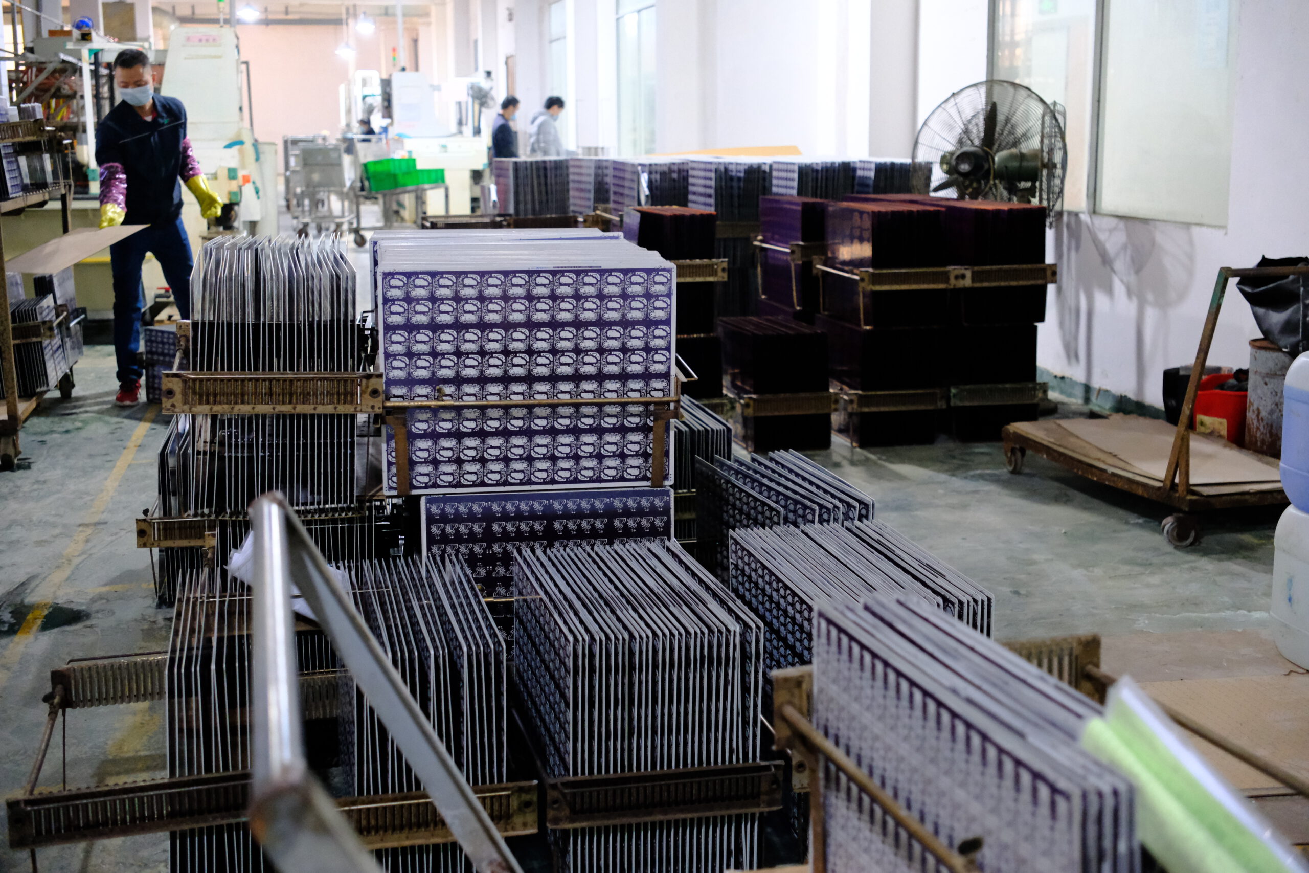
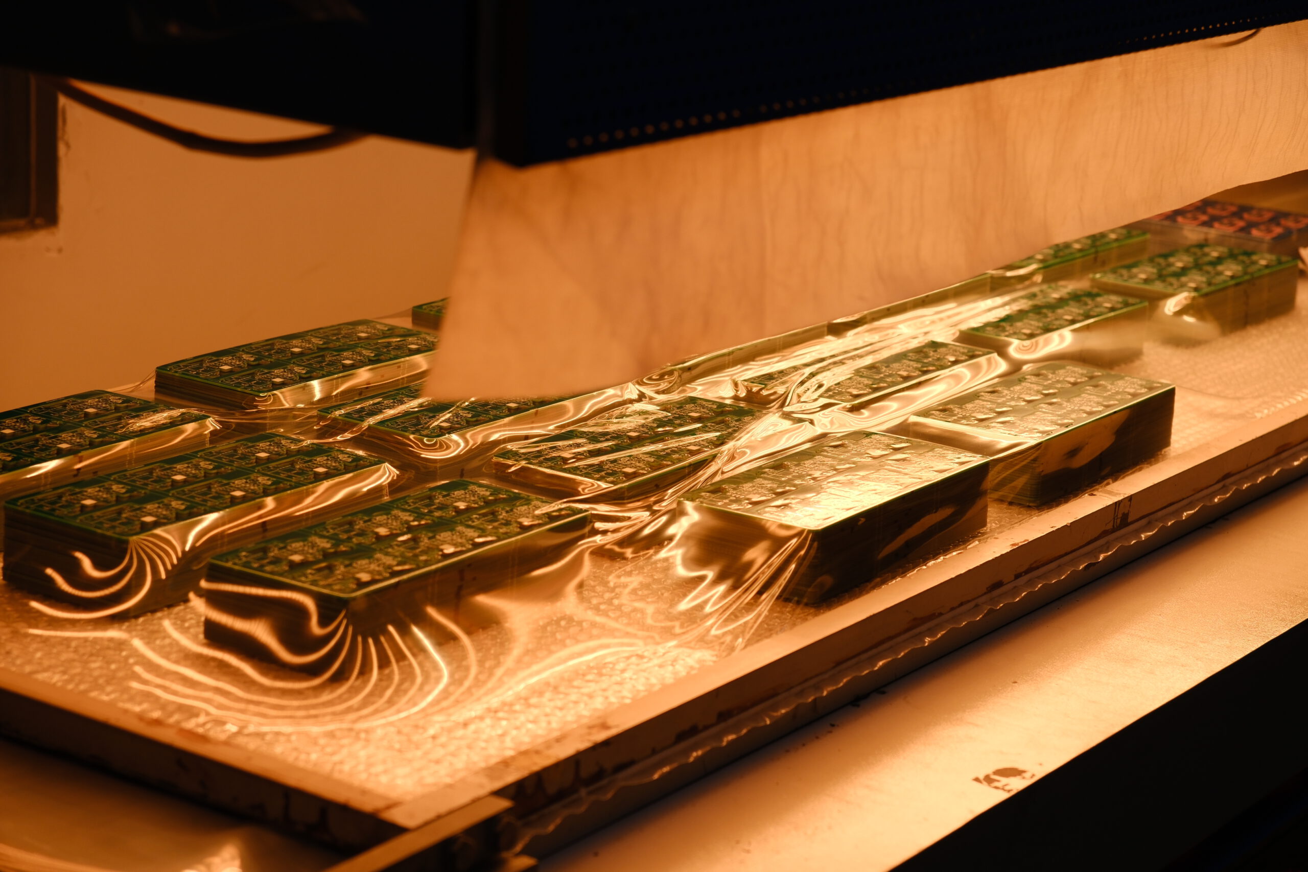
When you’re ready to bring your PCB design to life, your Gerber files are your golden ticket. These files are what manufacturers like BaiShun PCB use to turn your design into a real, physical board. But if they’re incomplete or incorrectly exported, it can lead to production delays or costly errors.
In this article, we’ll explain what Gerber files are, which layers are required, and how to package your files properly for a smooth quote and manufacturing process.
1. What is a Gerber File?
Gerber files are a set of standardized data files used to describe the layers of a printed circuit board (PCB). They tell the factory exactly how to fabricate your board — from copper traces and solder mask to drill holes and silkscreen text.
Most modern manufacturers (including BaiShun PCB) accept Gerber RS-274X, the most widely supported format across PCB CAD software like Altium, KiCad, Eagle, and EasyEDA.
2. Essential Gerber Layers You Must Include
Here’s a checklist of commonly required Gerber files for a standard 2-layer or multilayer PCB:
| File Type | Gerber Layer | File Naming Example |
|---|---|---|
| Top Copper | GTL (Gerber Top Layer) | project.GTL |
| Bottom Copper | GBL (Gerber Bottom Layer) | project.GBL |
| Top Solder Mask | GTS | project.GTS |
| Bottom Solder Mask | GBS | project.GBS |
| Top Silkscreen | GTO | project.GTO |
| Bottom Silkscreen | GBO | project.GBO |
| Mechanical/Outline | GML or GM1 | project.GML or project.Outline |
| Drill File | Excellon Format (TXT or DRL) | project.DRL or project.TXT |
| Readme (optional) | Design notes or assembly hints | Readme.txt |
✅ Tip: Always double-check your exported files in a Gerber viewer (such as Gerbv or Online Gerber Viewer) before submitting to avoid missing layers.
3. How to Export Gerber Files from Popular PCB Tools
Here’s how to generate your Gerbers in the most common EDA software:
-
Altium Designer: Use File → Fabrication Outputs → Gerber Files, and ensure RS-274X format is selected.
-
KiCad: Use the Plot function and include Drill Files. Export in .zip format.
-
Eagle: Use CAM Processor, load a 2-layer or 4-layer CAM job, and export all layers.
-
EasyEDA: Use Fabrication → Gerber Output, then download the .zip package directly.
4. Best Practices Before You Submit
To ensure quick quoting and faster turnaround, follow these file preparation tips:
-
🔒 Use consistent file naming across layers.
-
🧩 Compress all files into a single
.zipfolder. -
🔍 Double-check orientation and layer alignment in a viewer.
-
📐 Include a board outline (critical for cutting).
-
✅ Mention special requirements (like impedance control, copper thickness, or surface finish) in a readme or email.
-
📩 Email or upload directly to BaiShun’s quote system with a subject like:
“[Quote Request] 6-layer ENIG board for IoT device”
5. What Happens After You Submit Your Gerber?
At BaiShun PCB, once we receive your Gerber package:
-
📥 We run a pre-production DFM (Design for Manufacturability) check.
-
📊 You’ll get a quote within 24–48 hours, with production time and pricing.
-
🛠️ Once confirmed, your job enters our manufacturing pipeline with full QC control.
✅ Conclusion
Preparing Gerber files doesn’t have to be a headache. By following best practices, you’ll avoid delays, improve accuracy, and get your PCBs made faster and better.
Whether you’re designing for telecom, EVs, medical devices, or AI hardware, BaiShun PCB is ready to help — from first quote to final delivery.
📎 Need a quote now?
👉 [Click here to send us your Gerber files] or email: hello@jxbsdlkj.com
Share this article

Written by : bs.pcb
Follow us
A quick overview of the topics covered in this article.
Latest articles
April 21, 2026

April 21, 2026
")